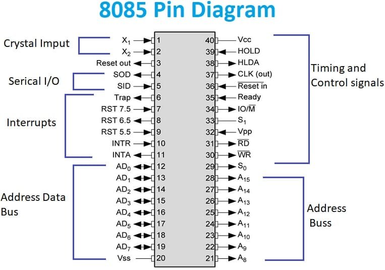
In this course, we will study the Pin Diagram of 8085 Microprocessor and its description.
Post credit: Pin Diagram of 8085 Microprocessor
What is the 8085 Microprocessor Pin Diagram?
The 8085 pin diagram consists of 40 pins of the microprocessor. The pins can be categorized into six groups-address and data bus, control signals, status signals, power supply, and serial input/output ports.
8085 Pin Diagram in Microprocessor
X1 AND X2
This is the first pin in the 8085 Pin Diagram in Microprocessor. The x1 and x2 represent the crystal oscillator which will provide frequency for the microprocessor.
Address Bus (A8-A15)
This is the second pin in the 8085 Pin Diagram in Microprocessor. The address bus pins range from A8 to A15 and these pins do the data transfer only.
Address Bus (or) Data Bus (AD0-AD7)
This is the third pin in the 8085 Pin Diagram in Microprocessor. The address bus pins or data bus pins range from AD0 to AD7, and these pins are called multiplexing lines that can do both addresses as well as data transfer.
Address Latch Enable (ALE)
This is the 4th pin in the 8085 Pin Diagram in Microprocessor. It is an active high signal. It represents the status of data lines (AD0-AD7). If the value is positive then it indicates that the address is going in the lines and if the value is negative then data is travelling in the lines.
Status Signal (IO/M)
This is the 5th pin in the 8085 Pin Diagram in Microprocessor. It tells us whether the address is intended for memory or input/output. In the case when we get a positive signal it represents that we have got i/o read or i/o write and when we get a negative signal it represents memory activation.
Status Signals (S0-S1)
This is the 6th pin in the 8085 Pin Diagram in Microprocessor. The status signals S0, and S1 give different functions as well as status based on their status.
- 01 then the operation will be HALT.
- 10 then the operation will be WRITE
- 10 then the operation will be READ
- 11 then the operation will be FETCH
RD
This is the 7th pin in the 8085 Pin Diagram in Microprocessor. The RD is an energetic low signal and it is used for controlling the microprocessor READ operation. When the RD pin goes small then the 8085 microprocessor understands the information from the I/O device or memory.
WR
This is the 8th pin in the 8085 Pin Diagram in Microprocessor. It has the power to control the microprocessor’s write operations. When the WR pin goes small the data will be written to the I/O device or memory.
READY
This is the 9th pin in the 8085 Pin Diagram in Microprocessor. The READY pin is for ensuring whether a device is set for accepting or transferring data. When the pin is high the device is ready for transfer, if it is not then the microprocessor stays until this pin goes high.
HOLD
This is the 10th pin in the 8085 Pin Diagram in Microprocessor. The HOLD pin specifies when any device is demanding the use of an address as well as a data bus.
HLDA
This is the 11th pin in the 8085 Pin Diagram in Microprocessor. It is the response signal of HOLD and is used to specify whether this signal is obtained or not. This signal will go low after the implementation of HOLD demand.
INTR
This is the 12th pin in the 8085 Pin Diagram in Microprocessor. This is an interrupt signal, and the priority of this among the interrupts is low. This signal can be allowed or not allowed by the software. The 8085 microprocessor completes the instruction which is being executed when the INTR pin goes high and recognizes the INTR signal and progresses it.
INTA
This is the 13th pin in the 8085 Pin Diagram in Microprocessor. INTA stands for interrupt acknowledgement. Whenever an interrupt signal comes, then it should be recognized by INTA. It is an active-low signal that is for zero it will process and for one it won’t.
RST 5.5, RST 6.5, RST 7.5
This is the 14th pin in the 8085 Pin Diagram in Microprocessor. These are the restart maskable interrupts or Vectored Interrupts which are used for the insertion of an inner restart function repeatedly. All these interrupts are maskable.
TRAP
This is the 15th pin in the 8085 Pin Diagram in Microprocessor. TRAP is a non-maskable interrupt, and it doesn’t allow or stop a program. TRAP has maximum precedence between interrupts. The priority order is TRAP, RST 5.5, RST 6.5, RST 7.5, and INTR.
RESET IN
This is the 16th pin in the 8085 Pin Diagram in Microprocessor. It is used to reset the program counter toward zero. It also rearranges interrupt enable as well as HLDA flip-flops (FFs).
RST (RESET) OUT
This is the 17th pin in the 8085 Pin Diagram in Microprocessor. It will reset all the devices connected to the microprocessor.
X1 X2
This is the 18th pin in the 8085 Pin Diagram in Microprocessor. X1, and X2 terminals that are associated with the exterior oscillator for generating the required as well as appropriate operation of a clock.
CLK
This is the 19th pin in the 8085 Pin Diagram in Microprocessor. Sometimes CLK signal has to be generated from microprocessors that can be used in favour of other peripherals or else other digital integrated circuits. This is offered with a CLK pin.
SID and SOD
This is the 30th pin in the 8085 Pin Diagram in Microprocessor. These two pins are used for serial data communication. In the serial input data, the information is uploaded into the 7th bit of the accumulator while RIM instruction is performed. RIM(Read interrupt mask) verifies whether the interrupt is covered or not covered. In the serial o/p data the output of the data is sent toward the 7th bit of the accumulator whenever an instruction of SIM is performed.
VSS and VCC
This is the 31st pin in the 8085 Pin Diagram in Microprocessor. VSS is a ground pin whereas Vcc is a +5v pin.


